View the series
View the series
Film for consultation only
© CNRS Images - 2008
Reference
1982
New technologies for lithography
Series title
Nanosciences and NanotechnologiesThis film derives from the Nanosciences and Nanotechnologies DVD.
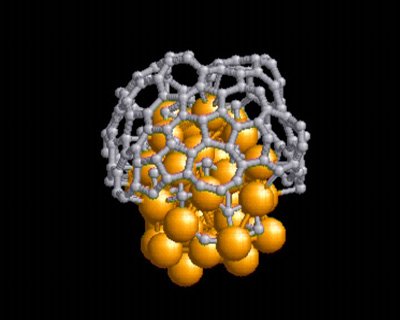
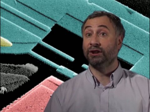
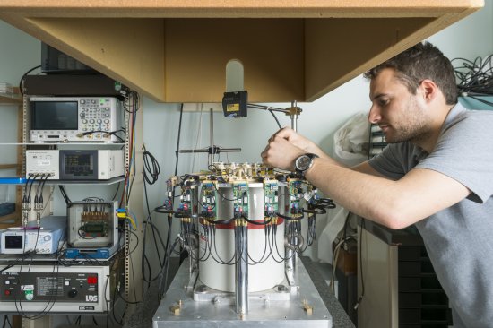
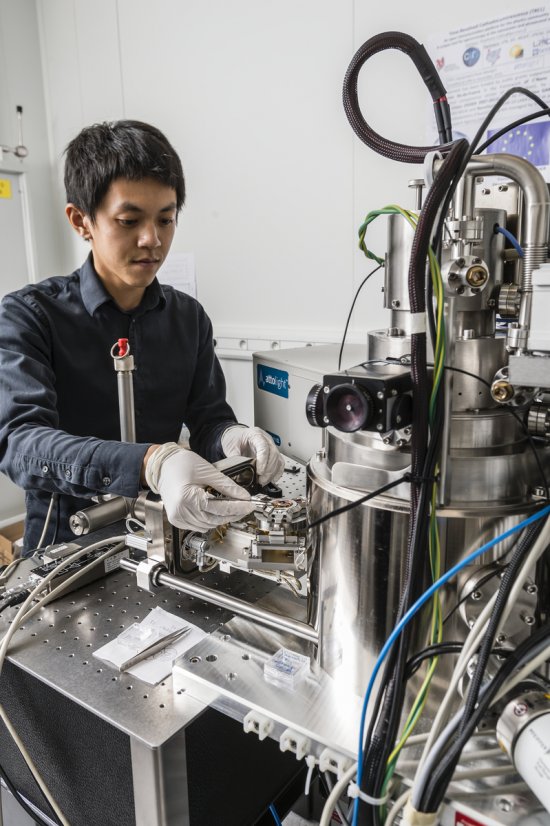
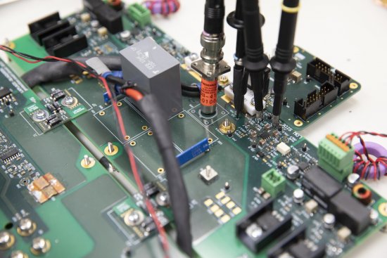
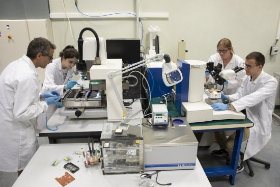
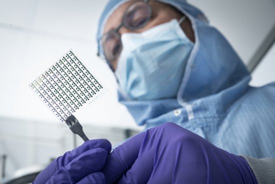
LPN research teams (photonics and nanostructures laboratory, Marcoussis) study the electrical and optical properties of the nano-objects they design and manufacture.
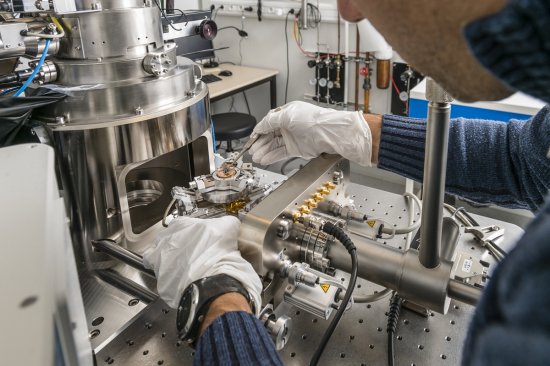
These nano-objects are made of various semiconductor materials and must be manufactured in clean rooms because the slightest dust particles could disrupt the operation of the devices obtained.
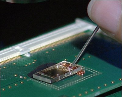
The first manufacturing step is lithography and, in the case of LPN, often electronic lithography because of its high resolution. Electron beams draw the patterns of objects in an electron-sensitive resin. After development, the resin will allow a template to be obtained by metal deposition. The last step will be engraving the patterns through the mask holes.
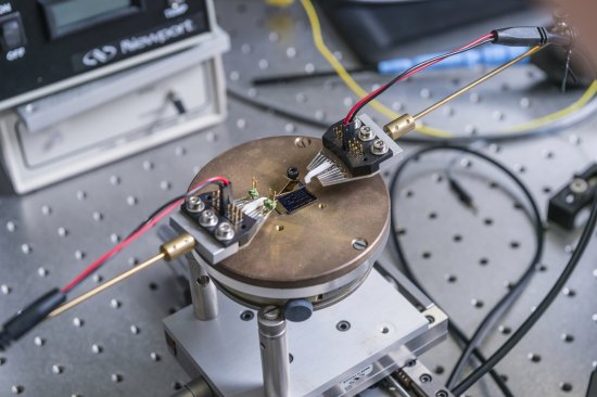
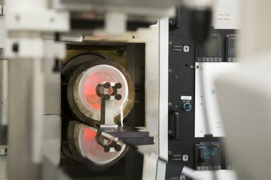
Very thin layer deposition techniques are molecular beam epitaxy and organometallic vapour phase epitaxy.
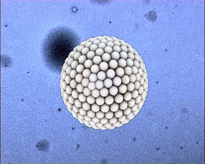
One structure often used is called a quantum dot. It consists of micro-pillars of semiconductor layers. First a stack of layers is made by successive epitaxies, then circular nickel studs are obtained at the top of this stack by lithography. These studs will be used as a template for reactive ion etching. They protect against engraving and cylindrical pillars are obtained under the studs.
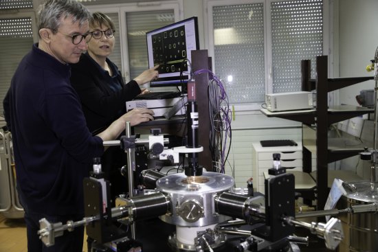
Electrically or optically energized quantum dots release photons. At the LPN, they make it possible to create sources of entangled photon pairs.
Duration
00:08:00
Production year
Définition
SD
Color
Color
Sound
Sound
Version(s)
French
International version
Original material
Video DV Cam
Add to my selection
Terms of use
The use of media visible on the CNRS Images Platform can be granted on request. Any reproduction or representation is forbidden without prior authorization from CNRS Images (except for resources under Creative Commons license).
No modification of an image may be made without the prior consent of CNRS Images.
No use of an image for advertising purposes or distribution to a third party may be made without the prior agreement of CNRS Images.
For more information, please consult our general conditions