Production year
2012

© Cyril FRESILLON/CNRS Images
20120001_1122
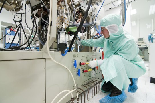
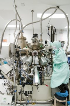
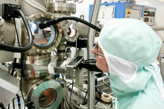
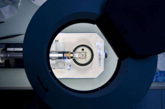
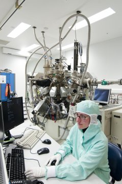
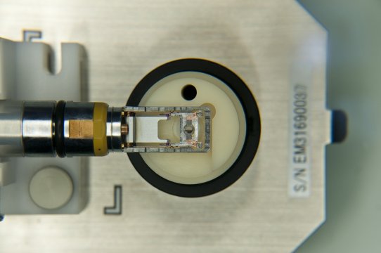
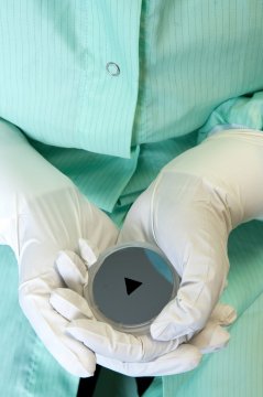
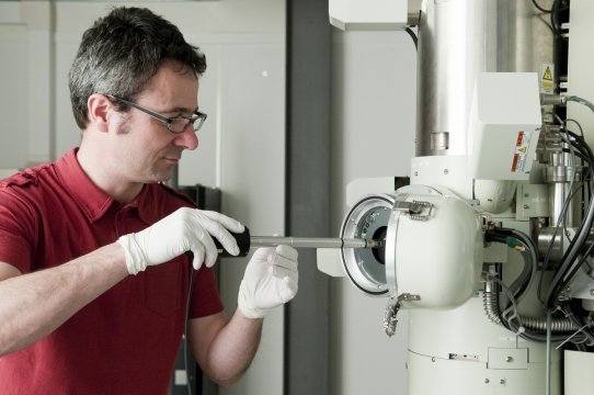
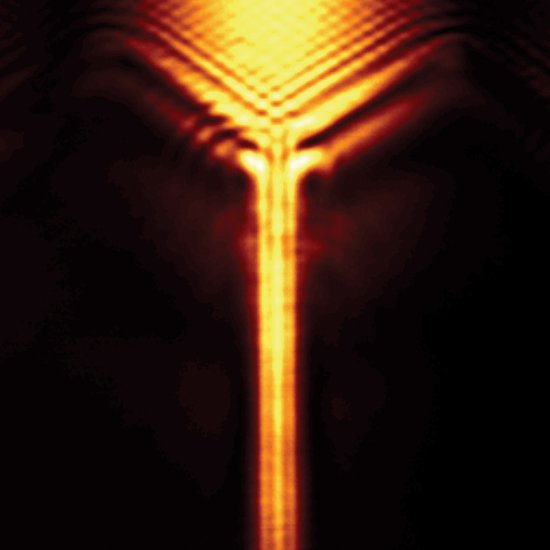
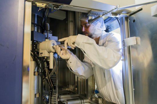
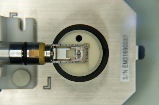
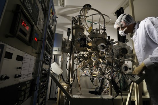
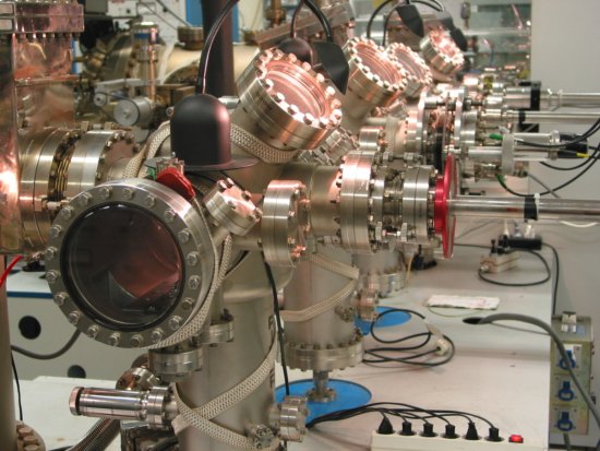
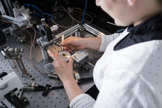
Transfert d'un échantillon, un substrat de semiconducteur III-V (GaAs arséniure de gallium ou InP phosphure d'indium), dans un bâti d'épitaxie par jets moléculaires. Après son dégazage, l'échantillon est transféré dans la chambre de croissance. Cette chambre est munie de 11 sources de matériaux élémentaires (aluminium, gallium, indium, azote, phosphore, arsenic, antimoine, silicium, carbone) pour l'élaboration de composés semiconducteurs III-V et leur dopage. Les échantillons ainsi élaborés servent à réaliser des dispositifs pour l'électronique et la photonique.
The use of media visible on the CNRS Images Platform can be granted on request. Any reproduction or representation is forbidden without prior authorization from CNRS Images (except for resources under Creative Commons license).
No modification of an image may be made without the prior consent of CNRS Images.
No use of an image for advertising purposes or distribution to a third party may be made without the prior agreement of CNRS Images.
For more information, please consult our general conditions
2012
Our work is guided by the way scientists question the world around them and we translate their research into images to help people to understand the world better and to awaken their curiosity and wonderment.