Only available for non-commercial distribution
© CNRS - 2021
Reference
7335
C2N, Scultting Matter
In order to sculpt their materials on the nanometric scale, when each speck of dust or infinitesimal vibration can compromise their work, physicists need cleanrooms that are insulated from all types of disturbances. An insight into the Centre for Nanoscience and Nanotechnology (C2N), where scientists have access to one of the largest such rooms in Europe, allowing them to produce materials with innovative properties.
Duration
00:09:47
Production year
Définition
HD
Color
Color
Sound
Sound
Version(s)
French
English
International version
Original material
Apple ProRes 422
Add to my selection
Terms of use
The use of media visible on the CNRS Images Platform can be granted on request. Any reproduction or representation is forbidden without prior authorization from CNRS Images (except for resources under Creative Commons license).
No modification of an image may be made without the prior consent of CNRS Images.
No use of an image for advertising purposes or distribution to a third party may be made without the prior agreement of CNRS Images.
For more information, please consult our general conditions
Transcription
C2N, sculpter la matière
Commentaire – voix off
Quelles sont les lois qui régissent le monde de l'infiniment petit ? Peut-on sculpter la matière à l'échelle nanométrique, celle du milliardième de mètre ? Depuis l'émergence des théories quantiques au début du 20eme siècle, la science tente de percer les mystères de ce monde à l'échelle de l'atome dans lequel les propriétés des matériaux changent du tout au tout. Ces recherches ont conduit à l'émergence des nanosciences et à la fabrication d'objets environ 10 000 fois plus petits qu'un cheveu.
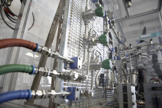
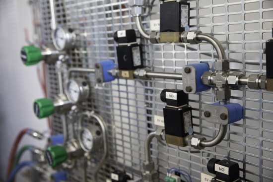
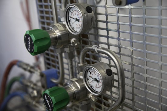
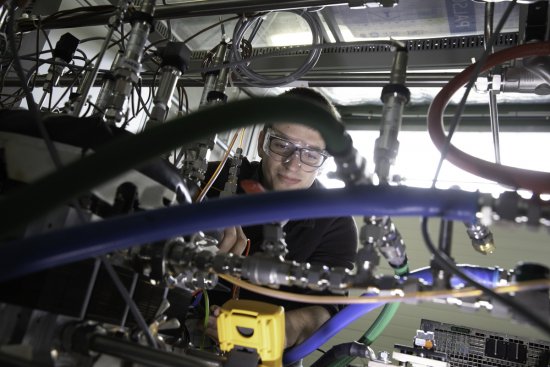
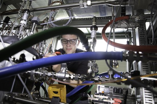
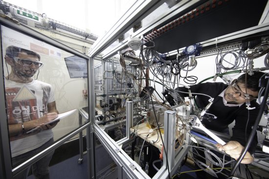
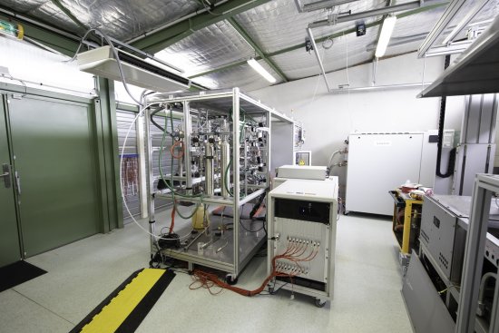
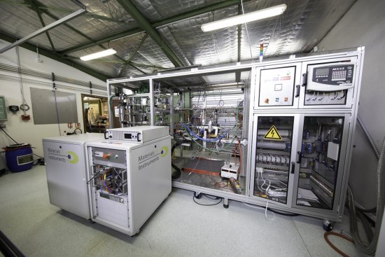
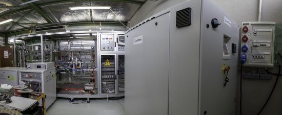
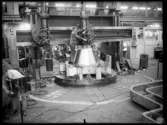
Pour interagir avec ce « nano-monde », les scientifiques ont dû imaginer des laboratoires et des machines pour réaliser des expériences avec une extrême précision. C'est dans cet objectif qu'a été conçu le C2N, le Centre de Nanosciences et de Nanotechnologies installé sur le plateau de Saclay en région parisienne. Un laboratoire qui accueille plus de 400 scientifiques spécialisés dans plusieurs domaines de recherche et qui héberge un outil rare : l'une des plus grandes salles blanches en Europe. Cette « centrale de nanotechnologie » de 3 000m2 contient tous les équipements de pointe nécessaire à la conception et à l'étude de composants fabriqués à partir de quelques milliers d'atomes. Acteurs académiques, étudiants et industriels peuvent s'y croiser.
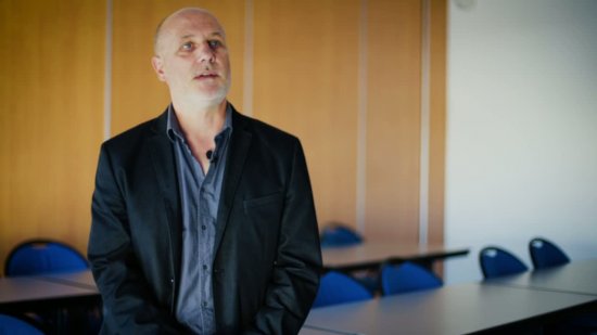
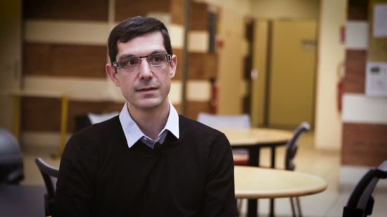
Giancarlo Faini, Directeur du C2N
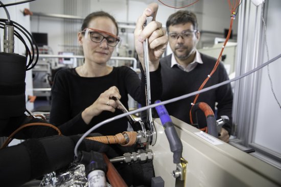
Les conditions de rigueur pour faire ces nano-objets sont extrêmes donc on doit s'affranchir de la poussière, on doit pouvoir filtrer ce taux de poussière, c'est pour ça qu'on appelle cela une salle blanche. C'est une des premières choses. La deuxième c'est tout ce qui peut perturber les instruments très sensibles qu'on utilise pour fabriquer, donc l'environnement électromagnétique. Et un grand ennemi aussi, les aspects de vibrations. C'est pour ça que la salle blanche est complètement découplé du reste du bâtiment. Vous imaginez quand on fait la lithographie on est en train de déplacer un faisceau de manière très précise pour pouvoir dessiner sur la surface, sur notre résine, un objet tout petit. Donc toute perturbation électromagnétique ou de vibration va créer des perturbations qui vont faire dévier le faisceau de quelques nanomètres par exemple… ce qui est très embêtant pour les objets qu'on veut réaliser.
Commentaire – voix off
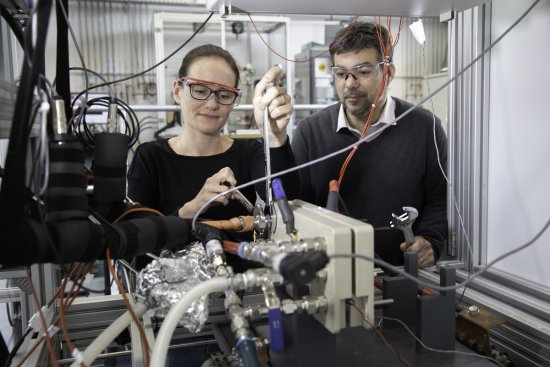
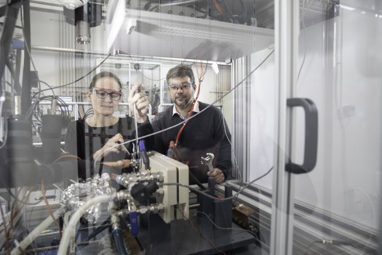
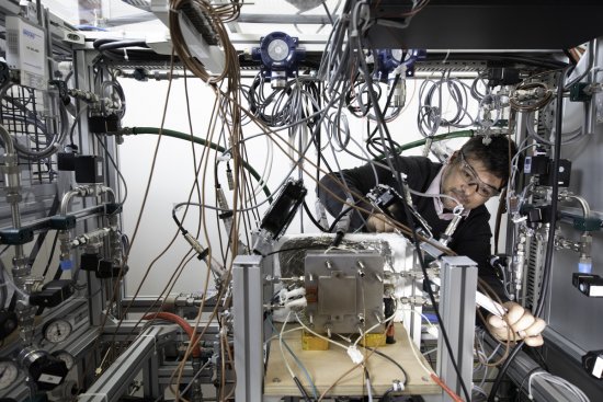
Plonger au coeur des matériaux réclame une importante capacité d'abstraction. A l'échelle nanométrique, impossible pour les chercheurs d'observer le résultat de leurs travaux à l'oeil nu. Ils doivent donc imaginer en amont le composant qu'ils souhaitent fabriquer, et préparer une recette à partir des matériaux de bases et des instruments à leur disposition. Dans ces locaux, des physiciens et des ingénieurs de recherche tentent de mettre au point les nanotechnologies de demain. Des composants qui pourraient permettre de faire voyager l'information à une vitesse extrêmement rapide, de résister à des conditions extrêmes ou encore d'offrir des propriétés physiques inédites.
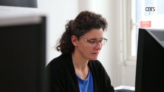
Laetitia Vincent, Physicienne
Les nanosciences sont vraiment basées sur la matière. La matière à l'échelle macroscopique donc visible, aura certaines propriétés et lorsqu'on réduit la taille ou la forme, en fait, de ces nano-objets on va obtenir de nouvelles propriétés donc c'est ça qu'on essaye d'investiguer dans les nanosciences. Alors il y a des propriétés qu'on découvre justement parce qu'on sculpte ces matériaux et on les caractérise, et puis il y a des propriétés que l'on recherche. Et notamment, Par exemple l'une des études qu'on mène dans notre équipe c'est qu'on essaye de faire croitre des cristaux à l'échelle nanométrique pour leur faire obtenir des propriétés optiques, donc d'émission de lumière, qu'ils n'ont pas dans une autre structure.
Commentaire – voix off
Pour assembler et sculpter ces nouveaux matériaux qui pourraient entrer dans la composition de futurs lasers, les chercheurs vont pouvoir compter sur l'ensemble des outils présents en salle blanche. Les paramètres environnementaux sont ici contrôlés en permanence, de même que les accès. Ces recherches peuvent en effet revêtir un caractère sensible tant en termes d'enjeux industriels que scientifiques.
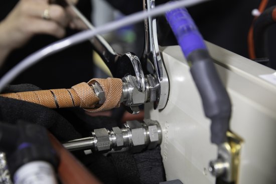
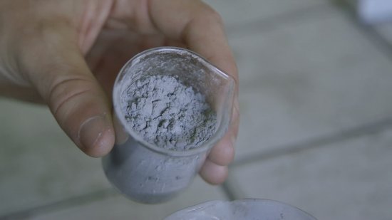
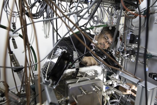
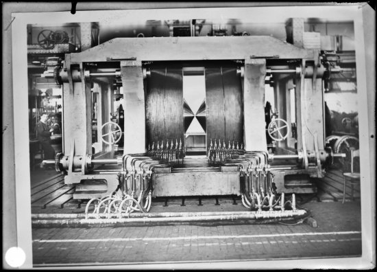
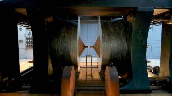
C'est dans ces salles que les chercheurs assemblent la matière, à partir de matériaux tels que ceux utilisés pour la microélectronique : le silicium, l'arsenic, le gallium…. Ces machines, appelées bâtis de croissance, permettent de créer des structures planes ou en volumes à partir d'atomes pulvérisés sur des surfaces. À l'intérieur de ces équipements règne un vide et une propreté absolue.
Laetitia Vincent, Physicienne
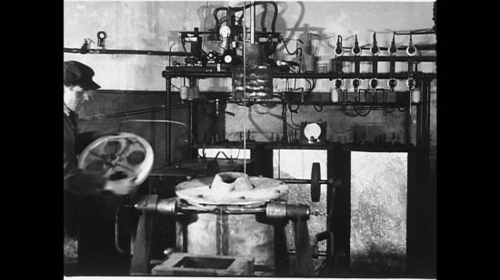
Dans cette machine on va faire des dépôts, c'est-à-dire qu'on va faire croitre nos cristaux atome par atome finalement. C'est une machine qui est sous vide, on rentre l'échantillon ici dans un sas et puis on va l'amener, toujours sous ultra vide, pour éviter toute contamination du substrat, on va l'amener dans notre gamelle qui est là-bas. Et dans cette gamelle on va venir injecter les gaz. Comme le substrat va être chauffé, les gaz vont craquer au niveau de la surface du substrat et les atomes vont venir se coller, s'absorber à la surface pour en fait veniuer créer des couches les unes après les autres.
Commentaire – voix off
Si de longs mois sont souvent nécessaires pour atteindre le vide propice à la bonne réalisation de la recette, la fabrication du composant ne prend que quelques heures. Mais comment observer le résultat de cette « croissance » de matière ?
Contrairement à la plupart des laboratoires spécialisés dans les nanosciences, le C2N offre aux chercheurs la possibilité de transporter leurs échantillons à travers les différentes étapes de leur élaboration au sein d'un même lieu. Dans ces salles, des microscopes électroniques permettent d'observer les composants qui ont été sculptés.
Ces images prisent à intervalles réguliers permettent d'observer la croissance de ces nouveaux matériaux sur le substrat. Lentement, les couches se superposent pour former de nouvelles structures qui pourront par la suite être façonnées et entrer dans la composition de nouveaux objets, cette fois visibles à l'oeil nu.
Ces études encore expérimentales dessinent pourtant peu à peu les ordinateurs et les outils de communication de demain.
Giancarlo Faini, Directeur du C2N
Il y a une synergie complète entre ce qui est la technologie, donc l'instrumentation, et la science. Quand on est en salle blanche le métier de l'ingénieur et du chercheur quand on est en train de faire des choses sont quasiment les mêmes, mais les motivations sont pas les mêmes. Donc, le scientifique va pousser le développement des technologies et les technologies, grâce à avoir des instruments de plus en plus précis etc. va en contrepartie faire avancer les sciences beaucoup plus rapidement. Pouvoir fabriquer des instruments de plus en plus précis permet de vérifier des lois qu'on ne pouvait pas vérifier avant ou de les contredire. De voir des choses donc au niveau expérimental qui vont à l'encontre de ce que l'on pouvait penser.
Commentaire – voix off
Si les outils du C2N permettent de mettre à l'épreuve les théories quantiques et d'observer les propriétés physiques des matériaux à l'échelle nanométrique, ils sont également utilisés dans des recherches appliquées aux enjeux très divers.
Une équipe s'intéresse ainsi à l'usage des nanotechnologies dans des applications médicales. Depuis plusieurs années, ces chercheurs tentent d'apporter une réponse innovante pour des patients atteints d'insuffisance respiratoire. L'objectif : développer un dispositif capable de fonctionner comme un véritable poumon artificiel. Cette équipe a dû concevoir en salle blanche une surface capable de simuler le parcours du sang humain à travers nos alvéoles pulmonaires. Il a fallu de nombreux essais pour parvenir à créer ce circuit de canaux gravés sur une surface de la taille d'un CD.
Julie Lachaux, Physicienne
Grâce à la micro-fluidique et à des techniques de micro-fabrication nous sommes capables ici de réaliser des dispositifs composés de micro-canaux dans lesquels circulent du sang et des micro-canaux dans lesquels circulent le gaz d'oxygénation, donc de l'air ou de l'oxygène pur. Et entre les deux canaux une fine membrane qui permet en fait l'échange de gaz c'est-à-dire l'apport d'oxygène dans le sang et le relargage du dioxyde de carbone. Donc ça permet de réaliser la fonction physiologique du poumon.
Donc là on voit que dans trois modules disposés les uns sur les autres on peut faire circuler un débit sanguin de 45ml par minute. En clinique il faudrait un débit d'un litre par minute, il faudrait donc une soixantaine de dispositifs empilés les uns sur les autres pour avoir un dispositif fonctionnel pour le corps humain.
Commentaire – voix off
La recherche et l'innovation dans le domaine des nanosciences et nanotechnologies développés au C2N sont le terreau de ruptures technologiques importantes à venir voir peut-être même de véritables révolutions scientifiques. L'avancée des moyens de communication actuels n'est que le premier pas vers une possible révolution industrielle.
Laetitia Vincent, Physicienne
Il y a plein de matériaux qu'on ne connait pas encore, plein de configuration de synthèse de matériaux si on s'en réfère en fait à la structure atomique. Il va y avoir plein de structures différentes empilées les unes sur les autres qu'on ne pouvait pas synthétiser autrefois et qu'on va être capable de synthétiser. C'est un nouveau monde, il y a plein de choses à explorer.
Commentaire – voix off
L'exploration de ce nanomonde est encore confrontée à de nombreux verrous théoriques que les outils présents en salle blanche pourraient permettre de faire sauter. Il appartient également d'ouvrir ces études à de jeunes chercheurs, en développant notamment la plateforme de formation actuellement en place au C2N.
Ce sont peut-être eux qui dessineront les contours du monde de demain en manipulant cet infiniment petit infiniment prometteur.