Production year
2021

© Riccardo GATTI / Laurent KORZECZEK / LEM / CNRS Images
20210137_0019
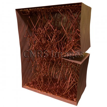
Throughout their use, materials are exposed to mechanical stress, which deforms and damages them. Such stress can be both mechanical, like an unforeseen impact, and thermal, such as a temperature change. This causes the formation and propagation of numerous defects within the material. However, the only way to understand, and therefore predict, their collective behaviour is to use numerical simulations. This micrometre-scale image, produced by digital modelling, shows a sample of copper that has cracked. A microstructure of dislocations – linear defects that cause plastic deformation, here seen resembling tangled spaghetti – was formed by the opening of the crack. This type of modelling can be applied to any crystalline material, and in particular to the metal alloys used in aircraft engines, as well as the semiconductors found in most electronic devices. This image is a winner of the 2021 La preuve par l'image (LPPI) competition.
The use of media visible on the CNRS Images Platform can be granted on request. Any reproduction or representation is forbidden without prior authorization from CNRS Images (except for resources under Creative Commons license).
No modification of an image may be made without the prior consent of CNRS Images.
No use of an image for advertising purposes or distribution to a third party may be made without the prior agreement of CNRS Images.
For more information, please consult our general conditions
2021
Our work is guided by the way scientists question the world around them and we translate their research into images to help people to understand the world better and to awaken their curiosity and wonderment.