Production year
2013

© Cyril FRESILLON/CNRS Images
20130001_1615
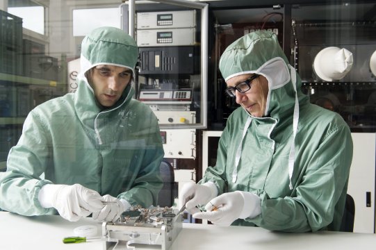
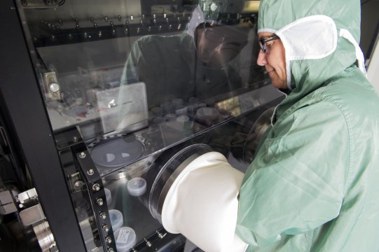
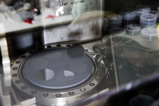
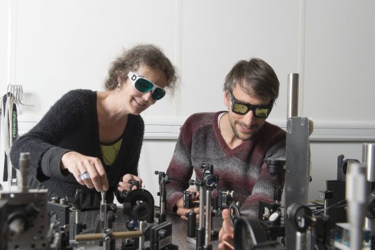
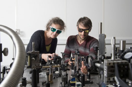
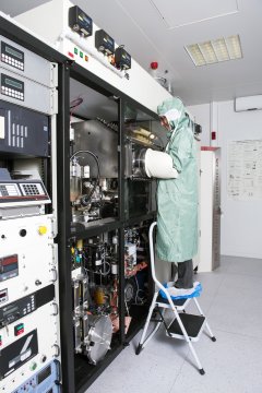
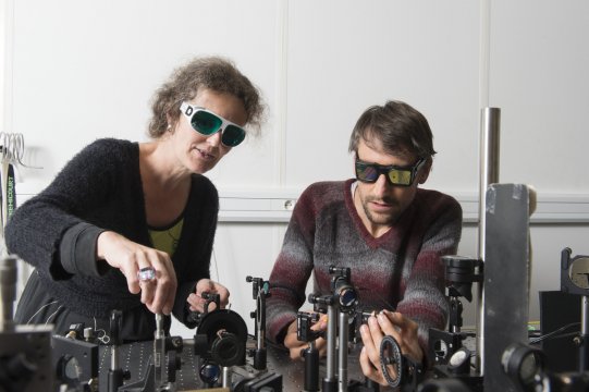
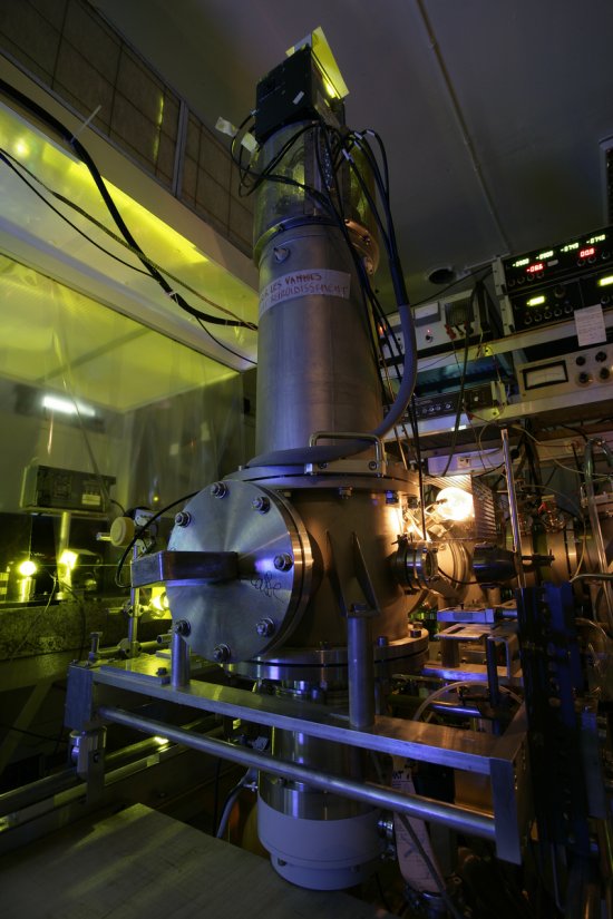
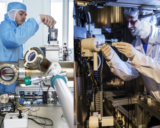
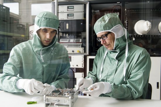
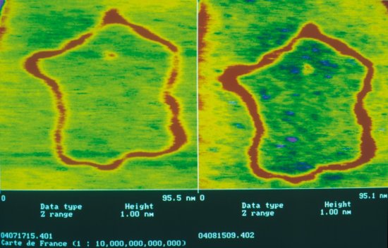
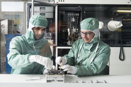
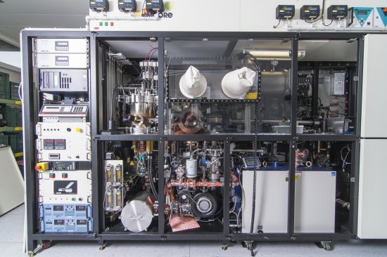
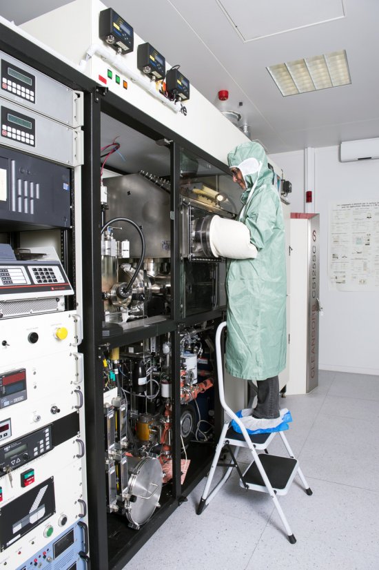
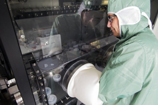
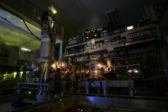
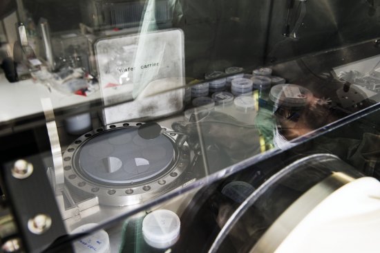
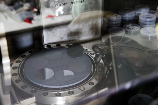
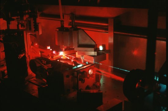
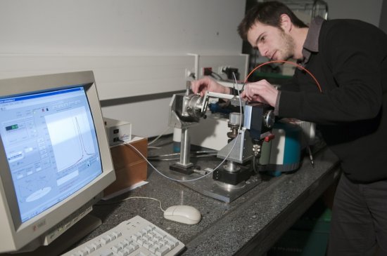
Positionnement d'un substrat de semiconducteur sur un porte-substrat. Il s'agit d'une étape technologique réalisée en salle blanche, après croissance de nanostructures semiconductrices sur un subtrat et avant l'étape de lithographie électronique. L'objectif est de mettre au point des composants nanophotoniques, pour obtenir de l'émission de lumière dans des dispositifs de plus en plus compacts.
The use of media visible on the CNRS Images Platform can be granted on request. Any reproduction or representation is forbidden without prior authorization from CNRS Images (except for resources under Creative Commons license).
No modification of an image may be made without the prior consent of CNRS Images.
No use of an image for advertising purposes or distribution to a third party may be made without the prior agreement of CNRS Images.
For more information, please consult our general conditions
2013
Our work is guided by the way scientists question the world around them and we translate their research into images to help people to understand the world better and to awaken their curiosity and wonderment.